Wtf is a “computer chip”? A CPU?
They mean smallest transistor
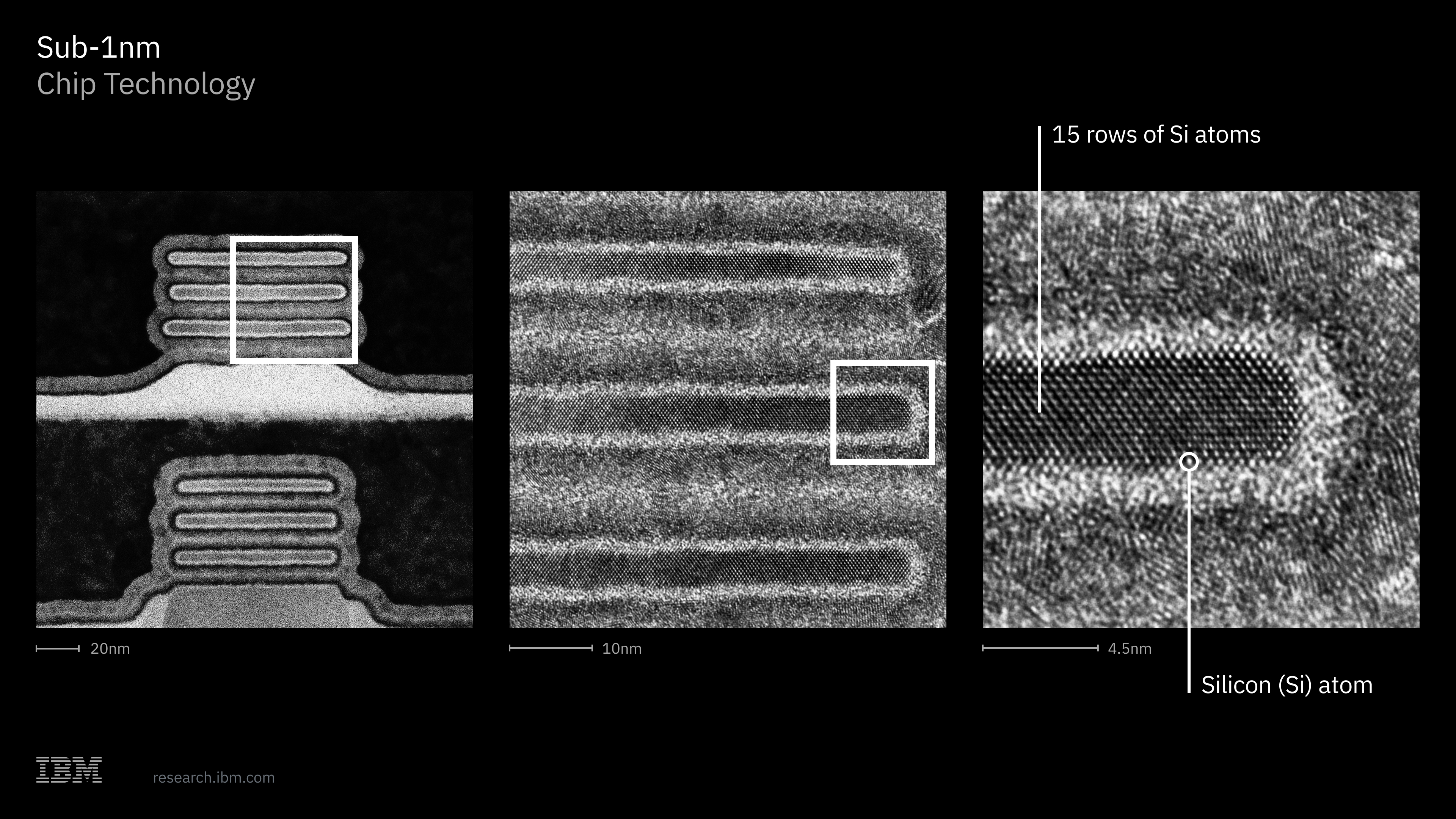
If that’s the smallest computer chip in the world, the hand must be tiny
We learned to shoot lightning at sand until it could do math.
Great quote. The sand:
Back when I was in college, IBM manipulated individual atoms to spell out “IBM”. I always wondered where that technology would end up!
https://en.wikipedia.org/wiki/IBM_(atoms)

They also made “a boy and his atom” https://en.wikipedia.org/wiki/A_Boy_and_His_Atom
Great! Just great. Now do the same to prices.
Imagine the size of spy cameras now…
Very cool. Stop lying by saying they are less than one nanometer.
I’d say it’s more an unfortunate consequence of confusing industry terminology. Sub-nanometer refers to the process, not the finished size of the chip. Smaller processes can fit more transistors in the same space.
They call it industry terminology, I call it false advertising. They could easily have used transistors per square mm.
The whole industry needs to be corrected.
The node sizes are backwards computed from the unit area of a one bit SRAM cell. It used to be the physical size of the smallest structure, e.g. a transistor gate.
I agree it’s highly misleading. Also, people forget that the original Moore’s law publication mention constant doubling time of transistors per area per unit of cost. So people keep pointing at multichip, thinned die stacking and 5 nm WSI like Cerebras to argue Moore scaling didn’t die a long time ago, but ignore costs.
The term “5 nm” does not indicate that any physical feature (such as gate length, metal pitch or gate pitch) of the transistors is five nanometers in size. Historically, the number used in the name of a technology node represented the gate length, but it started deviating from the actual length to smaller numbers (by Intel) around 2011.[3] According to the projections contained in the 2021 update of the International Roadmap for Devices and Systems published by IEEE Standards Association Industry Connection, the 5 nm node is expected to have a gate length of 18 nm, a contacted gate pitch of 51 nm, and a tightest metal pitch of 30 nm.[4] In real world commercial practice, “5 nm” is used primarily as a marketing term by individual microchip manufacturers to refer to a new, improved generation of silicon semiconductor chips in terms of increased transistor density (i.e. a higher degree of miniaturization), increased speed and reduced power consumption compared to the previous 7 nm process.
— https://en.wikipedia.org/wiki/5_nm_process
I agree that there should be a better way to describe these things. Why not describe the actual size like we used to. Quite strange.
Because while they weren’t shrinking in that aspect, other things were shrinking.
Its similar to how BMW decoupled their model numbers from displacement quite some time ago. Its where it sits in “the ranking”.
Mercedes too. An E300 used to have 300cm³ of displacement.
Still it’s better this way. People demanding huge displacement values for no fucking reason when technology has long moved on are among the dumbest on the planet.
Unfortunately a large part of marketing is people believing that others do not wish to be informed about such things. They just want to see “number move in good direction.” The stats unfortunately prove that. Most marketing material now is basically lying through omission.
Still no harm in changing the way in which we refer to the process to something more representative. It could signify a shift in manufacturing and you could spin it as a positive thing in marketing (which would surely not be lying).